


SiC Packaging: A Complete Guide to Silicon Carbide Power Module Selection and Design Considerations
Silicon carbide (SiC) power devices have revolutionized high-power electronics, but their performance heavily depends on proper packaging. This guide helps design engineers, power electronics engineers, and R&D teams understand the critical aspects of SiC packaging technology, from thermal management to reliability optimization. Whether you're designing EV powertrains, industrial motor drives, or renewable energy systems, selecting the right SiC package directly impacts efficiency, thermal performance, and long-term reliability.
Table of Contents
- What is SiC Packaging and Why It Matters
- Key Technical Parameters for SiC Package Selection
- SiC Package Types: Comparison and Selection Guide
- Thermal Management in SiC Packaging
- Design Considerations and Common Pitfalls
- Reliability and Qualification Standards
- FAQ
- Conclusion and Next Steps
1. What is SiC Packaging and Why It Matters
SiC packaging refers to the housing and interconnect technology that protects silicon carbide semiconductor dies while enabling electrical connections, thermal dissipation, and mechanical mounting. Unlike traditional silicon IGBTs, SiC MOSFETs and diodes operate at higher switching frequencies (up to 100 kHz or beyond), higher junction temperatures (175°C to 200°C continuous), and higher voltage levels (650V to 3.3kV). These extreme operating conditions place unprecedented demands on package design.
The packaging choice directly affects system-level performance in several ways. First, parasitic inductance in the package limits the maximum practical switching speed of SiC devices. Even a few nanohenries of lead inductance can cause significant voltage overshoot and ringing at 100 kHz switching frequencies. Second, thermal resistance from junction to case (Rth(j-c)) becomes the dominant factor in determining power density and derating requirements. Third, the package must withstand thousands of thermal cycles without delamination or bond wire fatigue, as SiC devices enable wider temperature swings than silicon equivalents.
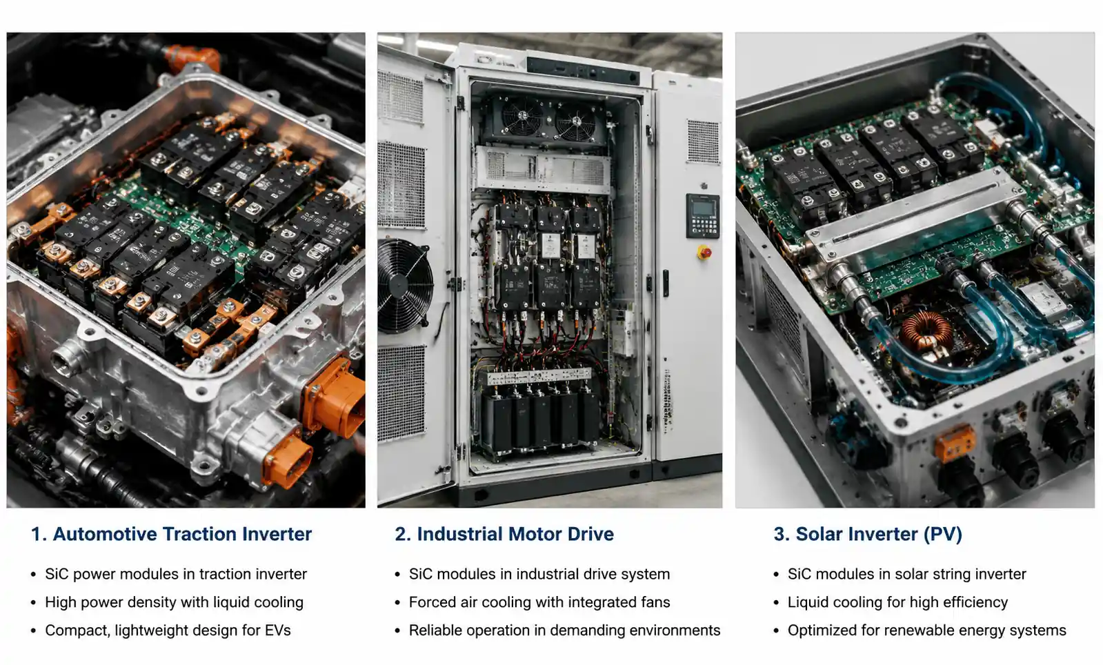
In automotive traction inverters, for example, a poorly chosen package can limit power density by 30-40% compared to an optimized solution. In renewable energy applications, package-induced failures account for approximately 60% of field failures in power electronics. Understanding the trade-offs between package types, thermal performance, and reliability is therefore essential for any engineer working with SiC technology.
2. Key Technical Parameters for SiC Package Selection
When evaluating SiC packages for your application, several technical parameters require careful analysis. The thermal resistance from junction to case (Rth(j-c)) typically ranges from 0.15°C/W to 0.5°C/W for discrete devices, and 0.02°C/W to 0.1°C/W per switch position in power modules. Lower thermal resistance enables higher current ratings and better efficiency at elevated ambient temperatures.
Package parasitic inductance is critical for high-frequency switching applications. Total loop inductance (including package leads, internal bond wires, and PCB traces) should be minimized to reduce voltage overshoot. Advanced packages achieve stray inductance below 5 nH, while traditional TO-247 packages may exhibit 15-20 nH. This difference translates directly into dv/dt capability and EMI performance.
Creepage and clearance distances determine voltage isolation capability. For automotive applications (800V battery systems), packages must provide at least 8mm creepage distance to meet safety standards. Industrial applications at 1200V require proportionally larger spacing. Package footprint and height affect power density in the final system. Half-bridge modules typically range from 62mm × 108mm (industry standard) to compact 45mm × 75mm designs for high-density applications.
Current rating must be derated based on actual thermal conditions. A 300A module at 25°C case temperature may only deliver 150A at 100°C case temperature, depending on Rth(j-c) and maximum junction temperature. Always verify current ratings at your actual operating conditions rather than relying on datasheet maximum values. Package lifetime is quantified through power cycling capability, typically specified as number of cycles to failure at a given delta-T junction temperature swing. High-reliability packages achieve 100,000+ cycles at ΔTj = 100°C.
| Parameter | Typical Range | Impact on Design | Priority Level |
|---|---|---|---|
| Rth(j-c) | 0.02 - 0.5 °C/W | Power density, cooling requirements | Critical |
| Stray inductance | 2 - 20 nH | Switching speed, voltage overshoot, EMI | Critical |
| Creepage distance | 8 - 25 mm | Voltage rating, safety certification | High |
| Package footprint | 45×75 to 140×190 mm | System power density | Medium |
| Current rating (Tc=100°C) | 50 - 800 A | Power handling capability | Critical |
| Power cycling capability | 10k - 500k cycles | Lifetime, warranty period | High |
| Operating Tj(max) | 150 - 175 °C | Derating requirements | High |
This parameter table provides the foundation for package selection. The relative importance of each parameter varies by application: automotive traction inverters prioritize power cycling and compact footprint, while renewable energy applications emphasize long-term reliability and cost per ampere. Note that achieving low stray inductance often requires trade-offs in current rating or footprint, requiring careful optimization during the design phase.
3. SiC Package Types: Comparison and Selection Guide
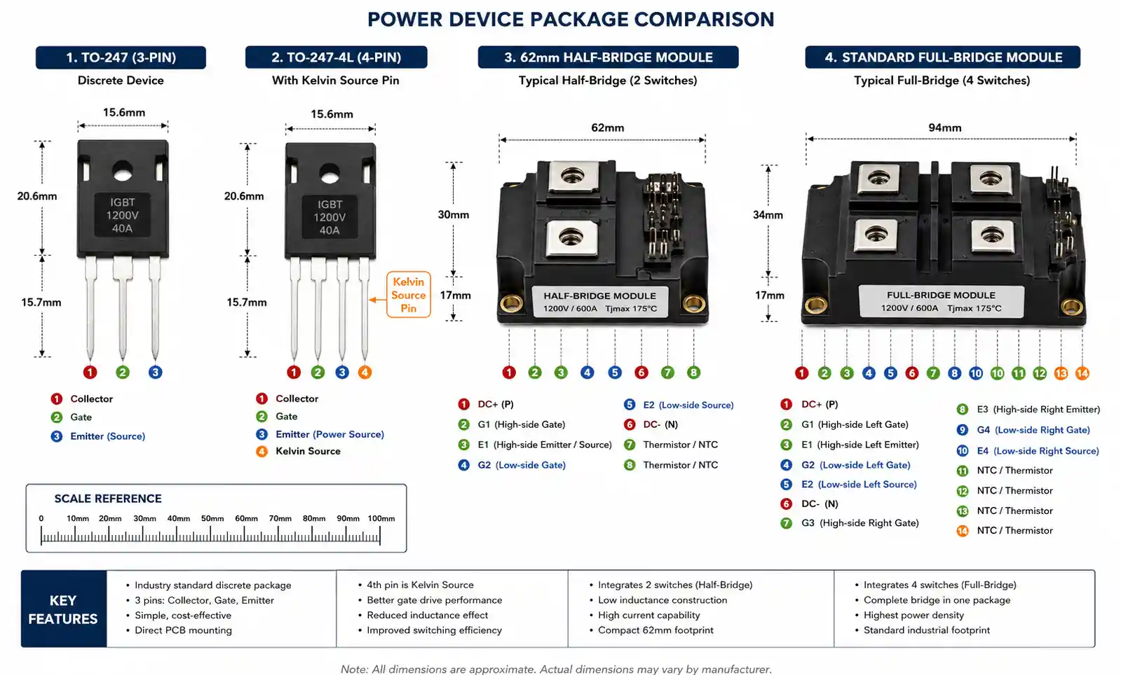
SiC devices are available in several distinct package families, each optimized for different application requirements. Discrete packages include TO-247, TO-220, and newer low-inductance variants like TO-247-4L. These packages suit applications from 10A to 150A with single-device implementations. The TO-247-4L variant adds a separate Kelvin source pin, reducing gate loop inductance by approximately 40% compared to standard TO-247.
Power modules integrate multiple SiC devices (typically half-bridge or six-pack configurations) into a single package with integrated gate drivers in some cases. Standard module footprints include 62mm packages for industrial drives and larger 140mm × 190mm modules for high-power traction applications. Modules offer several advantages: lower system-level inductance through optimized internal layout, integrated temperature sensors, and simplified thermal management through baseplate or direct-cooled designs.
Emerging package technologies include embedded die packages where SiC chips are embedded directly into PCB substrates, and press-pack packages for ultra-high reliability applications like HVDC transmission. Embedded packages achieve the lowest possible stray inductance (below 2 nH) but require specialized PCB fabrication. Press-pack designs eliminate bond wires entirely through pressure contacts, providing superior power cycling performance for applications requiring 500,000+ cycles.
| Package Type | Current Range | Stray Inductance | Best Applications | Relative Cost |
|---|---|---|---|---|
| TO-247 (3-pin) | 10 - 100 A | 15 - 20 nH | Low-power industrial, SMPS | 1x |
| TO-247-4L (Kelvin) | 20 - 150 A | 8 - 12 nH | High-frequency converters, on-board chargers | 1.2x |
| 62mm half-bridge module | 100 - 400 A | 5 - 10 nH | Motor drives, solar inverters, UPS | 3 - 4x |
| Standard full-bridge module | 300 - 800 A | 10 - 15 nH | Traction inverters, grid-tied inverters | 5 - 8x |
| Low-inductance module | 200 - 600 A | 2 - 5 nH | High-performance EV, fast-switching applications | 8 - 12x |
| Press-pack | 500 - 3000 A | 3 - 8 nH | HVDC, traction, ultra-high reliability | 15 - 25x |
For applications prioritizing switching frequency above 50 kHz, low-inductance modules or TO-247-4L packages are strongly recommended. The additional cost is offset by improved efficiency and reduced filtering requirements. Automotive applications should focus on modules with proven AEC-Q101 qualification and power cycling data above 100,000 cycles. Industrial and renewable energy applications can often use standard 62mm modules, which offer the best balance of cost, performance, and supply chain availability.
4. Thermal Management in SiC Packaging
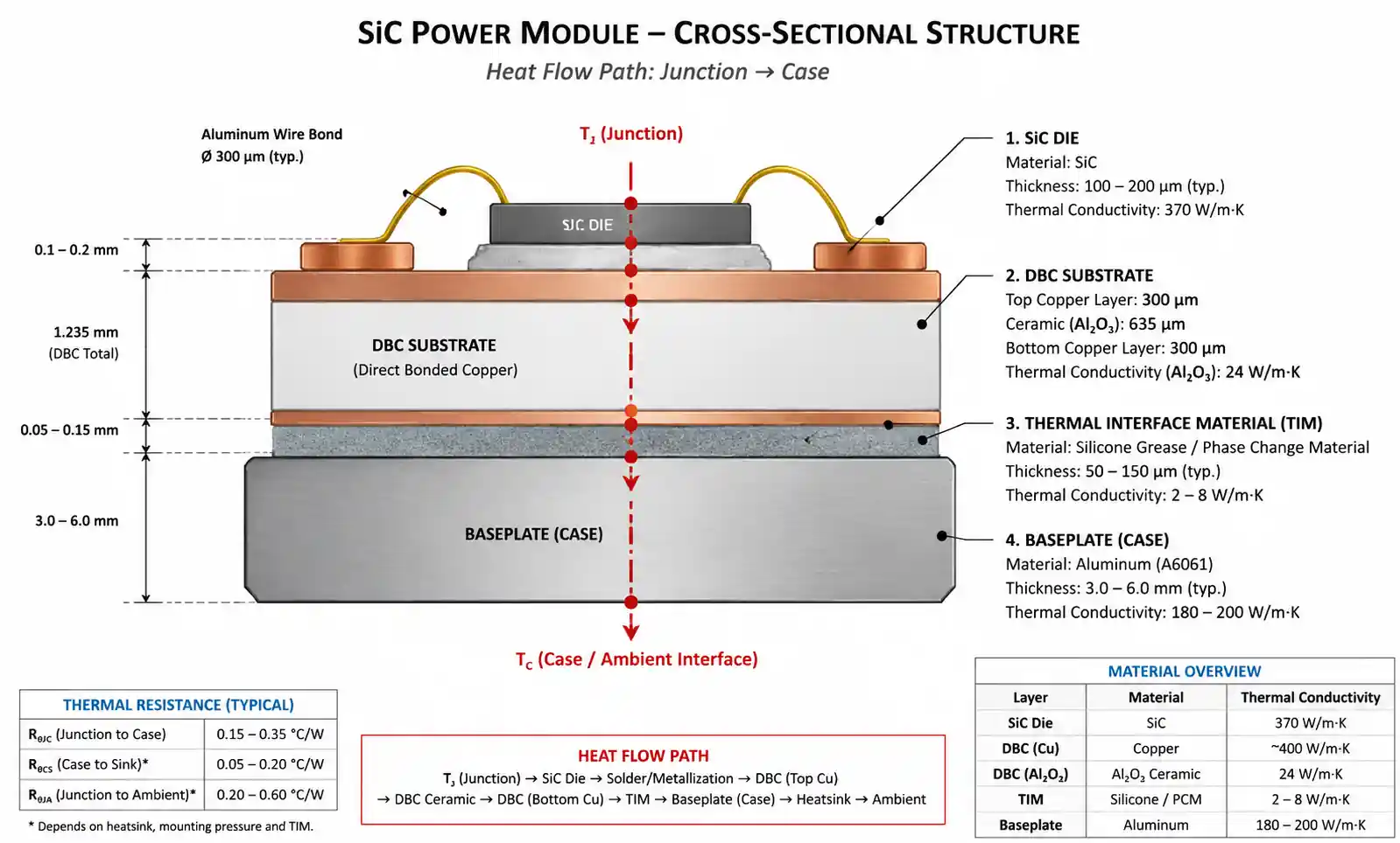
Effective thermal management starts with understanding the heat flow path from junction to ambient. In a typical SiC module, the die is soldered to a direct-bonded copper (DBC) substrate, which is then attached to a baseplate via thermal interface material or solder. The junction-to-case thermal resistance (Rth(j-c)) represents this path and typically dominates the total thermal resistance in well-designed systems.
For discrete packages, thermal resistance values range from 0.2°C/W (TO-247) to 0.4°C/W (TO-220) for a single die. Power modules achieve better performance through larger die attachment areas: a half-bridge module might achieve 0.05°C/W per switch position. Case-to-sink thermal resistance (Rth(c-s)) adds another 0.05 to 0.2°C/W depending on thermal interface material quality, mounting pressure, and surface finish. This means proper heatsink mounting is nearly as important as the package itself.
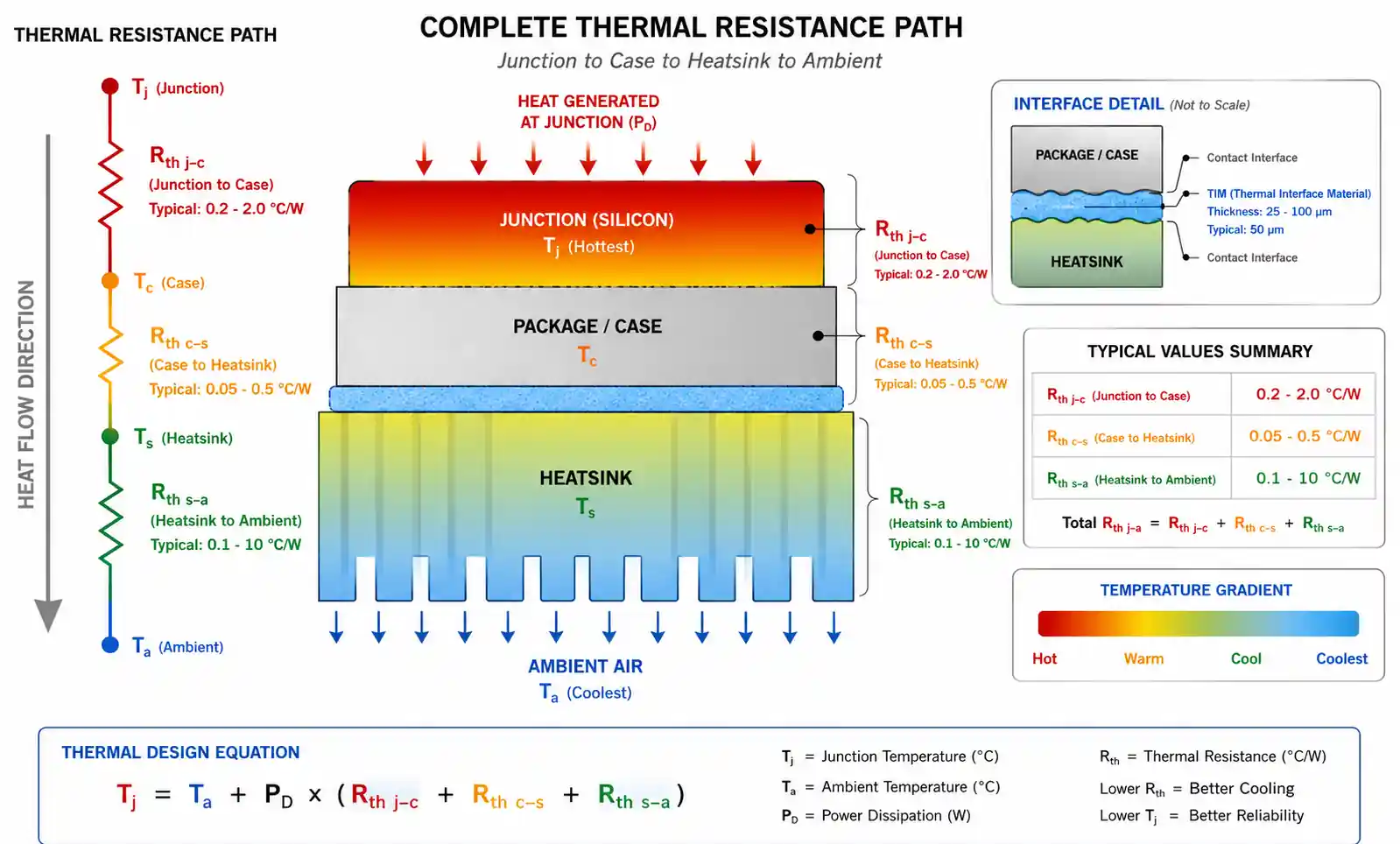
Junction temperature calculation requires accounting for both steady-state and transient thermal behavior. For continuous operation, Tj = Ta + (Rth(j-c) + Rth(c-s) + Rth(s-a)) × P_loss. However, pulsed operation allows thermal capacitance to absorb short-duration power peaks. This is particularly relevant for automotive duty cycles where peak power may be 3-4 times higher than continuous rating. Transient thermal impedance curves in the datasheet show how junction temperature rises over time scales from microseconds to seconds.
One common mistake is underestimating conduction losses in SiC devices. While switching losses decrease with SiC technology, on-state voltage drop still generates significant heat at high currents. A 1200V SiC MOSFET with 80mΩ on-resistance carrying 50Arms generates approximately 200W of conduction loss alone. When combined with switching losses and gate drive losses, total dissipation can easily exceed 250W per device, demanding careful thermal design.
| Cooling Method | Typical Rth(c-a) | Power Density | Cost Factor | Applications |
|---|---|---|---|---|
| Natural convection + heatsink | 2 - 5 °C/W | < 50 W/cm³ | 1x | Low-power industrial |
| Forced air cooling | 0.5 - 2 °C/W | 50 - 150 W/cm³ | 1.5x | Motor drives, SMPS |
| Liquid cold plate | 0.1 - 0.5 °C/W | 150 - 400 W/cm³ | 3 - 5x | Traction inverters, fast chargers |
| Direct liquid cooling | 0.05 - 0.2 °C/W | 400 - 800 W/cm³ | 8 - 15x | High-performance EV, aerospace |
| Two-phase cooling | 0.02 - 0.1 °C/W | > 800 W/cm³ | 20 - 30x | Extreme power density applications |
For most automotive traction applications, liquid cold plate cooling provides the optimal balance between power density and system complexity. Industrial applications below 50kW can typically use forced air cooling, while renewable energy installations often employ natural convection with appropriately sized heatsinks to eliminate fan failures. Always verify thermal design with worst-case ambient temperature, altitude (affects air cooling), and duty cycle conditions.
5. Design Considerations and Common Pitfalls
The most critical design consideration for SiC packaging is gate loop inductance minimization. The gate driver circuit must be placed as close as possible to the package gate pins, with ground return paths carefully managed. Gate loop inductance above 10 nH can cause instability in fast-switching SiC devices, leading to parasitic oscillation or false turn-on of complementary devices. Using four-pin packages with separate Kelvin source connections reduces gate loop inductance by providing a dedicated gate return path.
PCB layout around the package requires careful attention to power loop geometry. The DC link capacitor should be positioned to minimize the area enclosed by positive and negative current paths. For a half-bridge configuration, this means placing the DC capacitor directly adjacent to the package with wide, short traces. Each additional inch of trace length adds approximately 20-30 nH of inductance, which directly translates into voltage overshoot during turn-off transitions.
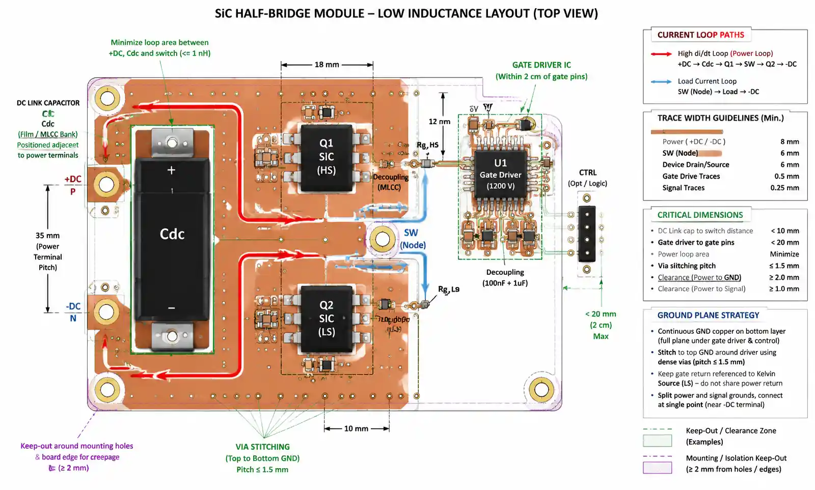
Parallel operation of multiple SiC devices demands precise matching of parasitic elements. Unequal stray inductance between parallel devices causes current imbalance during switching transitions, potentially leading to localized overheating and premature failure. If parallel operation is required, use devices from the same production lot, ensure symmetric PCB layout, and consider active gate drivers that compensate for device-to-device variations. In many cases, upgrading to a single higher-current device is more reliable than paralleling multiple lower-current devices.
Voltage overshoot during turn-off is proportional to stray inductance and di/dt: V_overshoot = L × di/dt. With SiC devices achieving di/dt values of 10-50 kA/µs, even 10 nH of inductance produces 100-500V overshoot. This must be accounted for in device voltage rating selection. For an 800V DC bus application, use 1200V devices rather than running 1000V devices at their limit. The additional margin prevents avalanche breakdown during transient conditions.
| Common Pitfall | Consequence | Prevention Strategy |
|---|---|---|
| Excessive gate loop inductance | Oscillation, false turn-on, shoot-through | Use 4-pin packages, minimize gate driver distance |
| Poor DC link capacitor placement | Voltage overshoot, EMI, device overstress | Position capacitors within 2cm of power terminals |
| Inadequate thermal interface material | Hot spots, premature failure | Use high-quality TIM, ensure proper mounting torque |
| Underestimating switching losses | Thermal runaway, unexpected derating | Calculate losses at actual switching frequency and voltage |
| Ignoring power cycling in design | Field failures after 1-3 years | Select packages with proven cycling data > 100k |
| Insufficient creepage distance | Partial discharge, insulation breakdown | Verify distances against IEC 60664-1 standards |
A frequently overlooked issue is gate resistor selection. While lower gate resistance reduces switching time and losses, it increases di/dt and dv/dt, exacerbating EMI and voltage overshoot. The optimal gate resistance represents a compromise: typically 2-10Ω for SiC MOSFETs depending on device size and application requirements. Always verify gate resistor power rating, as peak gate currents can exceed 5A during fast switching.
6. Reliability and Qualification Standards
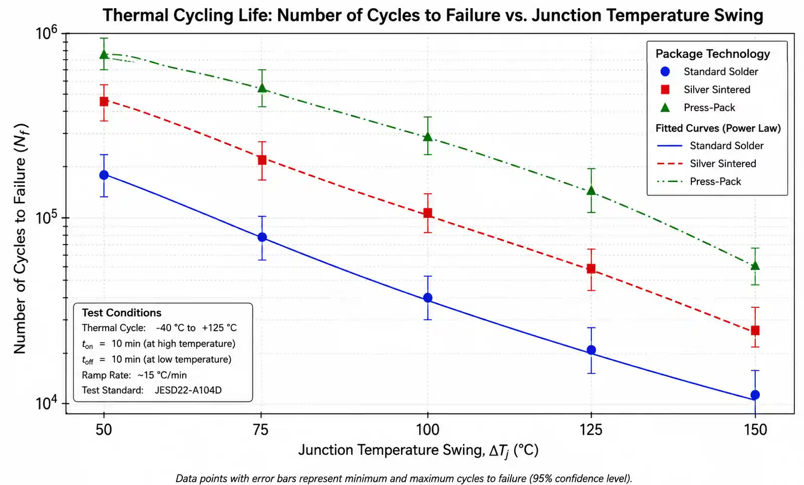
SiC package reliability centers on three main failure mechanisms: bond wire fatigue, solder layer delamination, and dielectric degradation. Bond wire fatigue occurs due to coefficient of thermal expansion (CTE) mismatch between aluminum wire and silicon carbide die. Each thermal cycle causes microscopic plastic deformation at the bond interface. After 10,000 to 100,000 cycles (depending on ΔTj), cracks propagate and resistance increases, eventually leading to open circuits.
Modern high-reliability packages address bond wire fatigue through several approaches. Silver sintering replaces traditional solder die attach, providing superior thermal cycling performance due to better CTE matching and higher melting temperature. Copper wire bonding offers better fatigue resistance than aluminum but requires special processes to prevent galvanic corrosion. Some advanced modules eliminate bond wires entirely, using copper ribbon interconnects or press-pack construction for applications requiring 500,000+ power cycles.
Automotive qualification follows AEC-Q101 standards for discrete semiconductors and AEC-Q200 for passive components, but power modules often require additional testing per manufacturer-specific requirements. Key tests include power cycling (minimum 50,000 cycles at ΔTj = 80-100°C), thermal shock (-40°C to 150°C, 1000 cycles), high-temperature reverse bias (HTRB), and humidity-temperature-bias (H3TRB) testing. Industrial applications typically reference IEC 60747 standards.
| Qualification Standard | Target Application | Key Tests | Typical Requirement |
|---|---|---|---|
| AEC-Q101 | Automotive (discrete) | Power cycling, HTRB, TC | 50k cycles @ ΔTj=80°C |
| AEC-Q200 | Automotive (modules) | Power cycling, thermal shock, vibration | 100k cycles @ ΔTj=100°C |
| IEC 60747-9 | Industrial power | Surge, MSL, thermal cycling | 10k cycles @ ΔTj=80°C |
| IEC 61287 | Railway traction | Power cycling, vibration, shock | 100k cycles @ ΔTj=125°C |
| MIL-STD-750 | Aerospace, defense | Extended temperature, radiation | 20k cycles @ ΔTj=150°C |
For mission-critical applications, request power cycling test data from the module manufacturer showing actual test conditions and results. Many datasheets provide only generic reliability estimates without supporting data. A trustworthy manufacturer will provide S-N curves (stress versus number of cycles to failure) and Weibull analysis showing failure distribution. This data allows accurate lifetime prediction based on your specific duty cycle and temperature profile.
Field reliability is strongly influenced by installation quality. Improper mounting torque can introduce mechanical stress that accelerates package cracking. Thermal interface material must be applied uniformly at the specified thickness, typically 50-200 microns. Exceeding maximum junction temperature even briefly can cause rapid degradation of gate oxide and metallization. Implementing temperature monitoring and protection in the control firmware is essential for achieving datasheet reliability projections.
7. FAQ
What is the difference between baseplate and base-less SiC modules?
Baseplate modules use a metal baseplate (typically copper or aluminum-silicon-carbide composite) attached to the DBC substrate, providing structural rigidity and a uniform thermal interface for heatsink mounting. Base-less modules eliminate the baseplate, directly exposing the DBC substrate for attachment to heatsinks. Base-less designs reduce thermal resistance by 0.02-0.05°C/W and package height by 3-5mm, improving power density. However, they require flat heatsink surfaces (< 50µm flatness) and careful mounting to avoid mechanical stress. Baseplate modules are more forgiving of thermal management system variations and are preferred for industrial applications where maintenance personnel may replace modules.
How do I calculate the required DC link capacitance for SiC packages?
DC link capacitance must supply ripple current during switching transitions while limiting voltage ripple. The minimum capacitance is C_min = I_out / (2 × f_sw × ΔV), where I_out is load current, f_sw is switching frequency, and ΔV is acceptable voltage ripple (typically 2-5% of DC bus). For a 400A, 20kHz inverter with 2% ripple on 800V DC bus, C_min ≈ 625µF. Additionally, low-ESL film capacitors (polypropylene or ceramic) must be placed near the module to handle high-frequency current components. Total DC link design requires analyzing both bulk energy storage and high-frequency decoupling requirements.
Can SiC packages operate at higher junction temperatures than rated?
While SiC semiconductor material can theoretically operate above 200°C, package materials limit practical junction temperature to 150-175°C continuous. Exceeding Tj(max) specifications degrades gate oxide reliability, accelerates metallization electromigration, and reduces power cycling lifetime. Brief excursions to 200°C during transients may be acceptable, but continuous operation above rated Tj(max) voids warranty and dramatically reduces expected lifetime. Always design thermal management to maintain junction temperature below maximum rating under worst-case conditions including maximum ambient temperature, altitude, and end-of-life thermal interface degradation.
What are the main differences between automotive-grade and industrial-grade SiC packages?
Automotive-grade packages undergo extensive qualification testing per AEC-Q standards, including 100,000+ power cycles, enhanced moisture sensitivity testing, and broader temperature ranges (-40°C to 150°C ambient). They typically use silver sintered die attach and copper wire bonds for superior reliability. Industrial-grade packages may use solder die attach and aluminum wire bonds with 50,000 cycle qualification, sufficient for stationary applications with controlled environments. Automotive packages also include stricter traceability requirements and manufacturing process controls to achieve near-zero DPPM (defects per million parts) failure rates required for safety-critical traction applications.
How does altitude affect SiC package thermal performance?
At higher altitudes, reduced air density decreases convective heat transfer by approximately 10% per 1000m elevation. This primarily affects forced air and natural convection cooling systems. At 2000m altitude, air cooling performance degrades by roughly 20%, requiring larger heatsinks or higher fan speeds to maintain equivalent thermal resistance. Liquid cooling systems are minimally affected by altitude since liquid density and thermal properties remain constant. Additionally, reduced air pressure lowers the partial discharge inception voltage, requiring larger creepage distances for high-voltage applications above 2000m elevation.
What testing should I perform to validate SiC package selection?
Begin with thermal verification using thermocouples or thermal cameras to measure case temperature under maximum load conditions. Verify that junction temperature calculated from case temperature and datasheet Rth(j-c) remains below Tj(max) with appropriate margin. Perform EMI testing per CISPR 25 (automotive) or CISPR 11 (industrial) to confirm that switching transients and parasitic resonances are within limits. Conduct accelerated life testing with 1,000-5,000 power cycles at your worst-case ΔTj to screen for assembly defects. For high-volume production, implement in-circuit testing of gate threshold voltage and on-state resistance to detect counterfeit or damaged devices before system integration.
Are there drop-in replacements for silicon IGBT modules using SiC?
Several manufacturers offer SiC modules with footprints compatible with standard IGBT modules (62mm, 140mm packages), allowing direct mechanical replacement. However, "drop-in" replacement requires gate driver modifications because SiC MOSFTs require different gate voltage levels (+15V/-4V typical) and higher gate drive current capability compared to IGBTs. Additionally, the faster switching speed of SiC demands reduced gate loop inductance and improved PCB layout that may not be present in existing IGBT designs. For optimal performance, expect to modify gate driver circuitry, DC link capacitor placement, and possibly PCB layout when upgrading from IGBT to SiC.
How do I handle long lead times for SiC power modules?
SiC substrate availability and complex packaging processes result in lead times of 16-52 weeks for power modules. Mitigate supply chain risk through several strategies: maintain strategic inventory of critical modules based on 6-12 month forecasts; design platforms with dual-source capability where possible, though exact drop-in replacements are rare; establish framework agreements with module manufacturers for committed capacity allocation; consider using discrete SiC devices in standard packages (TO-247) for prototypes with 8-12 week lead times, then transition to optimized modules for production. For new designs, engage module suppliers during architecture phase to align requirements with available products rather than specifying custom modules.
8. Conclusion and Next Steps
SiC packaging represents a critical enabler for next-generation power electronics performance. The choice between discrete packages and power modules, thermal management approach, and reliability qualification level must align with your specific application requirements. For automotive traction inverters, prioritize low-inductance modules with proven power cycling data exceeding 100,000 cycles and AEC-Q qualification. Industrial motor drives and renewable energy applications can leverage standard 62mm modules with forced air or natural convection cooling, optimizing for cost-effectiveness while maintaining adequate reliability.
The three most important parameters to verify for your application are: thermal resistance matching your power density targets, stray inductance compatible with your desired switching frequency, and power cycling capability meeting your lifetime requirements. If your application demands switching frequencies above 50 kHz or junction temperature swings exceeding 100°C, invest in advanced low-inductance packages or sintered die attach technology despite higher initial cost.
Before finalizing your package selection, download detailed datasheets including thermal models, power cycling curves, and layout guidelines. For high-volume applications, request samples and conduct thermal validation testing under your actual operating conditions. Many module manufacturers offer free simulation models (PLECS, LTspice) and application engineering support to assist with thermal and electrical design optimization.
If you need assistance with SiC package selection for your specific application, our team of field application engineers can provide detailed thermal analysis, reliability projections, and layout recommendations. Contact us to discuss your requirements and access our complete library of reference designs for automotive, industrial, and renewable energy applications.